Light switching device project (LSD)
Animation:
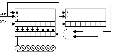
The data packet is clocked trough the shift-registers until the leading 1 is used as a trigger to compare the address field.
Only if the slave board has the address specified in the address field, the content in the shift register of the 74595 is buffered to the output registers.
i
At the next clock the leading 1 is used to flush the shift register to avoid that an address or a data bit is used as decoding trigger.
As you can see, it is fondamental that the leading 1 is detected well, and to be shure it is a good idea to send a sync-packet composed of only 0's (ideally 16 or more) preceding the real data packet.
Here you can find the complete circuit as I build it.
And here a list of all components used.
Back to the project page
|